News
Published over 4 years ago. See the latest and most current information on News.
During July, scientists at the US Department of Energy’s SLAC National Accelerator Laboratory advanced our understanding of next-generation computing technologies, after developing a way to look inside a tiny quantum electronic device. Researchers from SLAC, Stanford University, Hewlett Packard Labs, Penn State University and Purdue University, used a direct visualisation method which led to a surprise discovery; the existence of a short lived state that could be exploited for faster, more energy-efficient computing devices.
The findings were described as “a breakthrough in ultrafast technology and science” by SLAC scientist and collaborator Xijie Wang. “It marks the first time that researchers used ultrafast electron diffraction, which can detect tiny atomic movements in a material by scattering a powerful beam of electrons off a sample, to observe an electronic device as it operates.”
International Labmate caught up with Aditya Sood, a postdoctoral researcher at the Stanford Institute for Materials and Energy Sciences (SIMES) at SLAC, who explained further:
“Ultrafast electron diffraction has previously been used to understand how material structures respond on fast timescales to short pulses of light. However, it has never been used before to probe the dynamics of electric-field driven switching processes in a device. In general, there are hardly any experimental tools that can visualise atomic motions on fast timescales inside operating electronic switches, and correlate these atomic dynamics with changes in the electronic transport, so we decided to develop our own technique.”
For the experiment, miniature electronic switches were made of vanadium dioxide, a prototypical quantum material whose ability to change back and forth between insulating and electrically conducting states near room temperature could be harnessed as a switch for future computing. The material also has applications in brain-inspired computing because of its ability to create electronic pulses that mimic the neural impulses fired in the human brain.
The researchers used electrical pulses to toggle these switches back and forth between the insulating and conducting states while taking snapshots that showed subtle changes in the arrangement of their atoms over billionths of a second. Those snapshots, taken with SLAC’s ultrafast electron diffraction camera, MeV-UED, were strung together to create a molecular movie of the atomic motions.
“This ultrafast camera can actually look inside a material and take snapshots of how its atoms move in response to a sharp pulse of electrical excitation,” said collaborator Aaron Lindenberg, an investigator with the Stanford Institute for Materials and Energy Sciences (SIMES) at SLAC and a Professor in the Department of Materials Science and Engineering at Stanford University. “At the same time, it also measures how the electronic properties of that material change over time.”
Would it have been possible to observe the switching processes using any other type of camera or visual tracking?
“This would not have been possible to observe with a regular ‘camera’. To image atomistic dynamics, you need something that has a wavelength comparable to, or smaller than, the distance between atoms,” explained Aditya Sood. “Electron diffraction is a powerful probe of the atomic structure of materials because electron wavelengths are extremely small. When electrons transmit through materials, they produce interference patterns. By locating the peaks in the interference pattern, we can work backwards and deduce the positions of the atoms. Then, by shocking the electronic switch with an electrical pulse, we can understand how the atoms move by following changes in the interference pattern.”
SLAC scientist and collaborator Xiaozhe Shen, added: “The insulating and conducting states have slightly different atomic arrangements, and it usually takes energy to go from one to the other. But when the transition takes place through this intermediate state, the switch can take place without any changes to the atomic arrangement.”
Was the discovery of the intermediate state between insulating and conducting stages a complete surprise or had this been predicted? – if so what was this based on? How did you all feel when this was discovered/confirmed?
“The transient state of vanadium dioxide has been observed previously in light-driven experiments, but it was not known whether this transient state also forms under electrical excitation,” said Aditya Sood.
“It was very exciting when we first got this technique to work, and saw the first signs of voltage-induced structural changes in the diffraction patterns. There were many pieces of the experiment that had not worked for several months, and getting everything to fall into place was extremely satisfying!”
“This method gives us a new way of watching devices as they function, opening a window to look at how the atoms move. It is exciting to bring together ideas from the traditionally distinct fields of electrical engineering and ultrafast science.”
Can you elaborate a little more on the use of Vanadium dioxide for the switches and its associated mimicry of human neural firing responses - are any other materials being considered at this time or plans for development of such?
“Vanadium dioxide is a fascinating quantum material that is known to exist in two phases - these two states differ in their atomic arrangement, and have drastically different electrical conductivities. What is interesting from a device standpoint, is that one can go from the insulating to the metallic state simply by applying an electrical bias. This is quite appealing for electronics, but what has previously been unclear is what the pathway underlying this electrically-driven transition is and how fast it occurs. These are precisely the questions that our work seeks to address.
Previous work has shown that vanadium dioxide devices can be biased in a certain way to create repeated bursts of current that look a lot like neural impulses. In the future, we hope to use our technique to understand the atomic-scale structural dynamics occurring during these fast bursts.
Vanadium dioxide is a prototypical member of a category of materials called Mott insulators. It would be interesting to think about how our results on VO2 can be generalised to other members of this family, some of which may be relevant for computing applications.”
Although the intermediate state exists for only a few millionths of a second, it is stabilised by defects in the material and the team is investigating how to engineer these defects in materials to make this new state more stable and longer lasting. The research also offers a new way of synthesising materials that do not exist under natural conditions, allowing scientists to observe them on ultrafast timescales and then potentially tune their properties.
“We think there may be a pathway towards stabilising the transient phase on longer timescales by engineering disorder into the material. Exactly how this will be done is unclear at the moment, continued Aditya Sood. “If this can be achieved, it would allow Mott devices to switch purely electronically, i.e. without atomic structure rearrangement.”
Observation of functioning devices – are you following any other areas of research – or considering any research partnerships to develop these observation methods further?
It would be exciting to use our approach to look at the broader category of devices in which electric-field-induced transformations underlie functionality. This includes things like ionic memories and batteries. We now have a new way to connect how atoms move on ultrafast timescales with how electrical current flows in a device.
How can this approach be adopted ultimately by industry?
Can you see this developing into instruments for use at lead facilities, for example?
“At the moment, this is an advanced characterisation technique,” said Aditya Sood. “We hope that the insights gained through our approach can inform industry about pathways towards creating electronic devices with higher speed and energy-efficiency. Beyond the immediate implications for vanadium dioxide-based electronics, our work illuminates a new route (i.e. electrical-excitation) to create materials that don’t exist under normal conditions. This greatly expands the sandbox of materials science,”
Shriram Ramanathan, a professor at Purdue and collaborator on the project commented: “The results demonstrate the robustness of the electrical switching over millions of cycles and identify possible limits to the switching speeds of such devices,” said collaborator Shriram Ramanathan, a professor at Purdue. “The research provides invaluable data on microscopic phenomena that occur during device operations, which is crucial for designing circuit models in the future.”
MeV-UED is an instrument of the LCLS user facility, operated by SLAC on behalf of the DOE Office of Science, which funded this research.
The research team from the Department of Energy’s SLAC National Accelerator Laboratory, Stanford University, Hewlett Packard Labs, Penn State University and Purdue University described their work in a paper published in Science.
Citation: Sood et al., Science, 16 July 2021 (10.1126/science.abc0652)
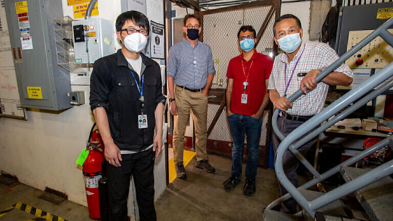
Laboratory Picture Credits: Jacqueline Orrell/SLAC National Accelerator Laboratory
ILM Guide 2026/27


.jpg)
.jpg)


-(1).jpg)
.jpg)


2.jpg)