News
Published over 10 years ago. See the latest and most current information on News.
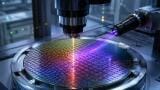
Scientists at Southampton’s Zepler Institute have successfully fabricated and characterised large-area 2D films of molybdenum disulphide (MoS2) at room temperature using a process which is scalable to any size wafer. Previously only commercially available in small flakes, these wafer-scale films pave the way for the large-scale manufacture of a wide variety of devices including flexible and transparent optoelectronics, gas sensors, memory devices and photovoltaics (PV).
Fabricated using ambient pressure chemical vapour deposition (CVD), the MoS2 films have an important advantage over other 2D materials like graphene: they enable the emission and detection of light and with exceptional carrier mobility is believed to be a strong contender for the next generation of electronics to take over as the silicon chip reaches its fundamental limits.
“Using flakes of MoS2, which are typically only a few hundred square microns in area, to make devices is impractical time-consuming and inefficient and do not provide a practical route to rapid prototyping and existing semiconductor fabrication protocols. For these new materials to be adopted in mainstream electronics, they must be compatible with the semiconductor processing lines used in the mass production of electronic chips.’ said Dan Hewak, Professor of Optoelectronics at the Zepler Institute. “Our expertise in novel thin-film fabrication coupled with our ultra-high purity raw material processing facility has enabled us to purify and synthesise large area films to a consistency and purity level not available commercially.”
The ambient pressure CVD process that Hewak and his colleagues have developed is an industrially-scalable and controllable deposition methodology and can be used to grow films on a variety of different substrates including plastic.
“We have also developed a technique for lifting these large-area films off the substrate they were grown on and depositing them onto a different substrate,” said Hewak. “This means the films can be put onto any material, opening up entirely new applications.”
Hewak and his colleagues are developing processes for the fabrication of a range of transition metal dichalcogenides and are part of the Chalcogenide Advanced Manufacturing Partnership (ChAMP) an EPSRC-funded partnership between five leading universities and 15 industrial partners dedicated to establishing the UK as a world leader in chalcogenide-glass technology.
ILM Guide 2026/27


.jpg)