Microscopy & microtechniques
Published over 17 years ago. See the latest and most current information on Microscopy & microtechniques.
In recent years the analysis of increasingly smaller structures in the scanning electron microscope (SEM) has become more important than ever. While SEMs have been able to resolve nanometer-sized features and produce according images for decades already, the issue is far more difficult for elemental analysis using energy dispersive X-ray analysis systems (EDS) on such microscopes. Bruker AXS Microanalysis has accepted this challenge and is proud to present solutions for its QUANTAX microanalysis systems that allow the SEM analyst to obtain elemental information on the nanometer scale.
Limiting factor for the spatial resolution of classical EDS is the comparatively large interaction volume of high energy electrons with bulk samples, which is in the range of several cubic microns. In principle there are two ways to overcome this limitation. The first is to reduce the interaction volume by analysing very thin layers that are transmitted by most electrons (100 nm), e.g. lamella prepared by focused ion beam (FIB). As only a minority of analysts will have access to such expensive equipment, Bruker has concentrated on the second option to reduce the interaction volume, which is to analyse at lower accelerating voltages, 1 – 5 kV instead of 20 – 30 kV. The lower energy electrons penetrate bulk samples not nearly as deep and so resolutions in the nm-range can be obtained. The prerequisite for this type of analysis is a SEM with field emission gun that can produce sufficient beam current at low accelerating voltages. This is far more common than FIB.
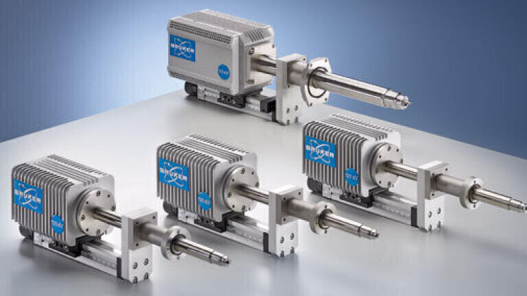
Due to the physics of EDS a simple reduction of the accelerating voltage is insufficient, far-reaching changes to analysis hardware and software are necessary. In addition to the already excellent energy resolution of its XFlash® silicon drift detectors, Bruker has adapted the detector design and materials to cause minimum interference with the “soft” low energy electron beam. Also we offer a number of geometrical optimisations to maximise the collection angle for X-rays, as far less are produced than at high energies.
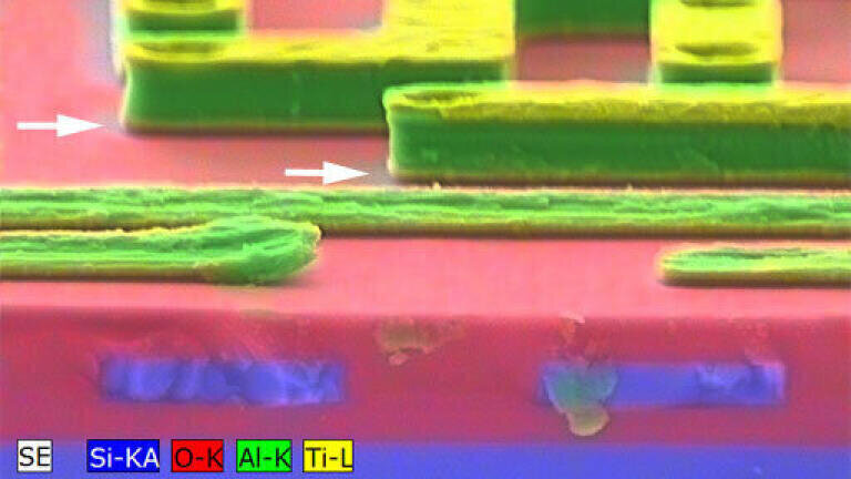
The ESPRIT software of Bruker’s QUANTAX systems has been modified to provide secure identification and deconvolution of the many overlapping element peaks in the low energy range. Thus enabling point analyses as well as nano-scale line profiles and 2D maps. It is also now possible to perform standards-based analysis on low energy spectra, providing reliable quantitative compositional information.
If you would like to learn more about the solutions Bruker has to offer in order to meet the challenges of nanoanalysis please view the recording of our recent webinar
ILM 51.6 Sept 2026




 Product directory