
Microscopy & microtechniques
Published over 15 years ago. See the latest and most current information on Microscopy & microtechniques.
Peltier cooled silicon drift detectors (SDD) were originally developed for space research to avoid the need of liquid nitrogen for cooling X-ray detectors. Figure 1 shows one of the first SDDs on Mars rover Spirit. Energetic alpha particles and X-rays from a curium-244 source are used here to illuminate Martian material. The SDD placed in the middle of the spectrometer in the inset on the upper right detects the resulting fluorescence. Compared to the simple diode design the SDD-signal readout is based on sideward depletion [1] assisted by a so-called drift field which guides the charge generated in the Si-device by the incoming X-rays towards a small readout node [2]. The reduced size of the readout area is the main reason for cooling by Peltier elements being sufficient in these devices. SDD technology allows much faster and more efficient data collection compared to the diodes cooled by liquid nitrogen. It was introduced for energy dispersive X-ray analysis (EDS) in scanning electron microscopy (SEM) more than a decade ago. In SEM the material of interest is exposed to an electron beam, which causes several types of interaction signals. Backscattered and secondary electrons are used to generate images of the sample. X-rays characteristic for excitations of particular states of the elements present in the sample are used for chemical analysis in EDS. Much effort has been invested into the optimisation of SDD-technology for a high quality element analysis. This includes the improvement of energy resolution, further noise reduction and speed of acquisition. After great success in SEM SDDs are now about to revolutionise EDS in transmission electron microscopy (TEM), which can deliver higher spatial resolution compared to SEM. Main aspects of SDD-EDS analysis in nanoscience are the topic of this contribution.
SDD technology for EDS
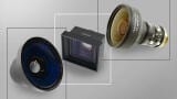
To facilitate any application in nm-size and below, whether molecular cages for drug delivery in the human body or a nanostructure for semiconductor industry, it is necessary to have means for nanoanalysis. To successfully realise nm-structures it is vital to be able to control the location of each element on nm and even atomic scale. EDS in combination with electron microscopy is a straightforward method to deliver this. Spatial resolution in SEM is improved by reducing the accelerating voltage of the electron beam to generate a smaller excitation volume. In TEM electron transparent samples are prepared so that the excitation volume is even smaller (Figure 2). The problem is though that in this case often the available beam current is smaller and due to this and the reduced excitation volume the genereted X-ray signal decreases. Therefore it is crucial to collect X-rays efficiently by covering a large solid angle around the sample. A good estimate for the solid angle Ω out of which data can be collected, measured in steradian [sr], is given by Ω [sr] = A (cos δ) / d2 [sr]. A is the detector area, d its distance to the sample and cosδ creates the projection of the detector area onto a part of the sphere around the sample. Therefore, δ is the angle between the detector surface normal and the line for the shortest distance between the detector centre and the sample surface. Geometric constraints in the microscope pole piece and ports often complicate the design of large solid angle detectors. At present the manufacturers are exploring various different designs. Side-entry detectors in SEM are mostly inserted at a suitable take-off angle between 30° and 45°. In TEM side-entry detectors are mostly inserted using the horizontal ports, which are generally the only ones available. In that case a particular effort is needed to realise a good take off angle for a good peak to background ratio in the spectra. The TEM side-entry detector has to be placed as high as possible above the sample without sacrificing solid angle. Multi-detector systems can offer much higher solid angles and better take-off angles than single side entry detectors [3]. Additionally they are combining this advantage with using small chip sizes, which compared to large area detector chips, need less cooling to attain good energy resolution, show less pile up and can be read out faster. Figure 3 shows an annular multiple chip detector, which reaches a solid angle of 1.4sr in SEM. For scanning TEM (STEM) integrated multi-detector systems were recently successfully developed [4].
ILM Guide 2026/27


.jpg)