Microscopy & microtechniques
Published over 13 years ago. See the latest and most current information on Microscopy & microtechniques.
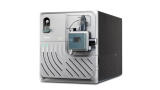
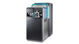
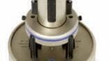
Bruker has announced the release of the Dimension Icon® SSRM-HR, a new atomic force microscope (AFM) configuration including the Scanning Spreading Resistance Microscopy (SSRM) module, designed specifically for high-resolution (HR) semiconductor characterisation. Integrating Bruker’s industry-leading Dimension Icon AFM platform with an environmental control system capable of 1ppm gas purity and high-vacuum control, the Dimension Icon SSRM-HR system provides vastly improved repeatability and spatial resolution in semiconductor carrier profiling.
“As our customers continue to improve their products to follow the semiconductor roadmap, higher spatial resolution electrical characterisation is a key requirement,” said David V. Rossi, Executive Vice President and General Manager of Bruker's AFM Business. “The new Dimension Icon SSRM-HR combines the leading productivity and large programmable stage of our top performance AFM platform with atomic resolution, and the most accurate carrier profiling optimisation to meet the specific demands of next-generation technology nodes.”
ILM Guide 2026/27