Microscopy & microtechniques
Published over 14 years ago. See the latest and most current information on Microscopy & microtechniques.
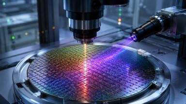
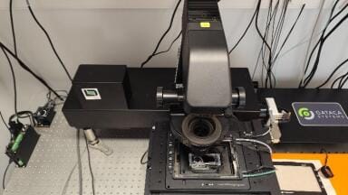
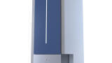
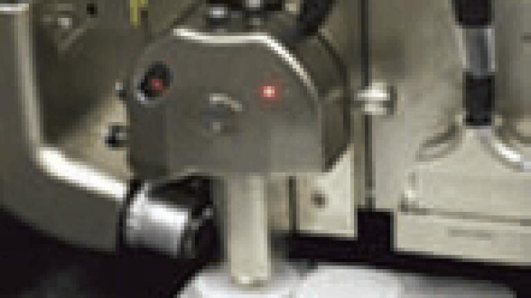
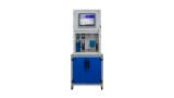
Bruker launched the Dimension EdgeTM PSS Atomic Force Microscope (AFM), a production-environment,
automated AFM specifically tailored for patterned sapphire substrate (PSS) metrology in high brightness lightemitting
diode (HB-LED) manufacturing. The Dimension Edge PSS is an easy-to-operate AFM that delivers
resolution far beyond traditional optical techniques while at the same time providing precise 3D profile
information to control the most advanced PSS processes. The system performs automated measurements and
data analysis on 2- to 6-inch wafers for production metrology applications, and offers a multitude of AFM
capabilities essential for LED R&D. The Dimension Edge PSS comes with Bruker’s exclusive AutoMETTM software
package, which greatly improves manufacturing productivity by fully automating AFM data collection and
analysis to provide a PASS/FAIL output for technician operation. “Driven by ever increasing performance and
cost demands, HB-LED manufacturers are looking to PSS technology to deliver critical process improvements, and the Dimension Edge PSS is instrumental in controlling these advanced processes,” said Mark R. Munch, PhD, President of the Bruker Nano Surfaces Division. “The Dimension Edge PSS provides rapid process feedback with its speed of measurement and unmatched precision and resolution.”
“With the release of the Dimension Edge PSS, Bruker continues to demonstrate its commitment to superior AFM performance and usability for both researchers and production environments,” added David V. Rossi, Vice President and General Manager of Bruker’s AFM Business. “The Dimension Edge PSS brings reliable AFM metrology into industrial applications, enabling the highest resolution measurements, and providing simple pass or fail measurement criteria for operator ease of use.”
The Dimension Edge PSS system utilises the strengths of the Dimension Edge AFM along with proprietary software to provide a turnkey production metrology solution for patterned sapphire substrate manufactures. These features combine to allow for technician level operation and a system ideal for production environments. Bruker’s automation software package is designed specifically to meet the production needs of HB-LED manufactures. The software can easily be configured to measure between one to nine wafers at multiple points per wafer, including automated data analysis and reporting, providing measurement details to the engineer and a PASS/FAIL indicator to the operator
ILM 51.5 July 2026


.jpg)


-(1).jpg)